Posted 2019/7/19
The SA series is configured by gathering various technologies for each model.
For example, while SA-250F6 has an input impedance of 50 Ω, its equivalent input noise voltage density is lower than thermal noise due to resistance of 50 Ω; in other words, it seems that SA-250F6 has the feature of negating the physical low. However, SA-250F6 is not a device that transcends the physical law; it was designed according to the existing physics (electrical and electronic engineering) theory. It was designed by using a technique called “active input impedance”, which plays an important role in supporting low noise (Figure).
Figure
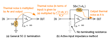
A simplified version of an amplifier with a typical input impedance of 50 Ω is shown in Figure (a). As for this method, 50 Ω thermal noise connected to the input is mixed with the signal, amplified, and output. For that reason, it is impossible for thermal noise to fall below that due to 50 Ω resistance, even in the case of an ideal amplifier without internal noise. The method for breaking through this “50 Ω wall” is the active input impedance method shown in Figure (b). Instead of removing the terminating resistors, input impedance is created with a negative-feedback (NF) resistor.
The SA-250F6 is an amplifier with a gain of 100 times (40 dB). Applying the active input impedance method compresses the influence of thermal noise to 1/10 or less compared with method (a), which uses a 50 Ω termination resistor as is.
This active input impedance method is essential for achieving an equivalent input noise voltage density that is lower than the 50 Ω thermal noise while maintaining an input impedance of 50 Ω.
Related keywords : Ultra low noise amplifier, LNA
